Making Miniaturization Possible with Advanced Electronics Assembly

The first mobile phones were literally the size of bricks and all they could do was make phone calls. Now think about the thin, lightweight mobile device that fits easily in your pocket today. In addition to making calls, it's a camera, a calculator and a calendar. It has email and text messaging. It's a calendar, a health tracker, a flashlight and more.
Thanks to the marvels of engineering, we've been able to continually shrink the size and weight of our devices while also making them more powerful. We call this miniaturization, and we use advanced electronic assembly processes to make it happen.
What is Miniaturization?
Miniaturization in electronic devices involves fitting more transistor nodes on a smaller integrated circuit (IC). The IC is then interfaced within its intended system or device so that, once assembled, the system can carry out the desired function. The technology is made tinier yet mightier.
Furthermore, device miniaturization aligns with Gordon Moore's 1965 prediction that "Cramming more components onto integrated circuits [would] lead to such wonders as home computers, automatic controls for automobiles and personal portable communications equipment." His prediction proved true, ushering in an era of technology that would vary from portable computers, smartphones and new medical devices to the Internet of Things and 5G wireless devices, as well as AR/VR and AI, all enabled by smaller yet more powerful computing systems.
Dreaming up these miniature technologies is one thing — the manufacturing process is quite another. Electronics manufacturers constantly innovate to overcome the challenges that come with interfacing smaller and more powerful electronic components.

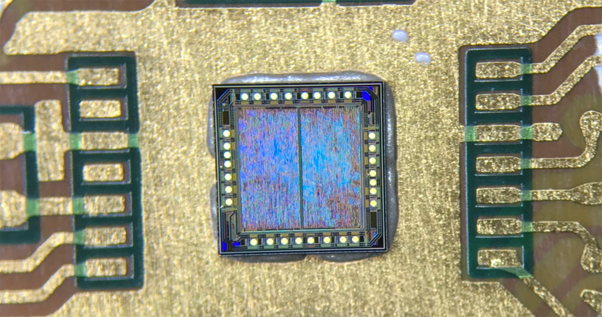
A tiny “bare die” chip is placed onto a circuit board using a precise advanced electronics assembly process
Miniaturization will change the world. But new advanced manufacturing processes, like advanced electronics assembly, are needed to tackle the challenges and embrace the promises of miniaturization.
Whether we are developing the next system-on-chip, or attaching it to a new device, advanced electronics assembly is the masterful combination of knowhow, precision and innovative processes that makes the devices dreamed up by our customers in a studio go into mass production and distribution across the world.
Doing More with Less: Downsizing with Ball Grid Arrays

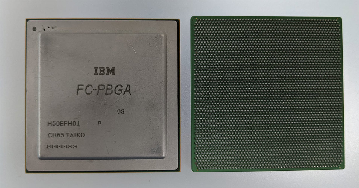
A ball grid array package showing the protected top and exposed underside gridded with solder balls. A grid pattern of solder balls is used where each ball becomes a connection between the circuit board and the BGA package. In this way, attaching a BGA on a printed circuit board reduces the overall system size while increasing the system performance.
One miniaturization technique is to develop integrated circuit packages in Ball Grid Arrays (BGAs). BGA designs enable large amounts of connections between the integrated circuit and printed circuit board - increasing the ability to route signals and therefore increasing the processing power of the system it is being assembled into.
BGAs also improve chip reliability and reduce overheating, as they allow for higher numbers of thermal channels and shorter signal travel lengths. Establishing more and better electrical connections make BGAs a key enabler in technology miniaturization.
Inherently, BGAs are a great way of integrating the plethora of sensing and response systems needed for applications such as autonomous vehicles. The Advanced Driver Assistance Systems (ADAS) that are critical pieces of autonomous vehicles require carefully calibrated sensors to gather the constantly changing information around a car as it travels down the road. According to Intel, "Autonomous vehicles will need the computing power necessary to fuse ~1gb/sec of information from various sensors to [output] safe decisions."
Of course, these systems must be rugged and reliable to meet safety standards. Research presented at the 2020 WCX SAE World Congress studied the performance of high-density BGAs under different thermal and vibrational situations, simulating conditions that an autonomous driving module would undergo when installed. Reliability is an important factor that directly impacts the design and therefore the assembly process we select to manufacture these systems.

Advanced Electronics Assembly
Advanced Electronics Assembly on a Miniature Scale
Beyond BGAs, another common miniaturization technique is the use of wafer level chip scale packages. Wafer level chip scale packages (WLCSPs) are essentially micro-scale ICs mass-created on a wafer that are later diced into an individual IC-containing die or chips of a few millimeters in length and width. Here, the connections are made of solid gold joints, either gold bumps or gold wire bonds. These gold joints maintain their reliability when they are as small as 30 microns in diameter; they can be placed a couple of microns apart.
As the size of transistor nodes goes down, chips can further be downsized without compromising performance. Sometimes their performance can even increase as they get smaller. These smaller transistor nodes are what enable the more robust system-on-chip (SoC), which can carry out more tasks with better performance.
Like BGAs, the connections on the IC die are usually accessed on the underside of the chip, but that can vary by chip design. This flexibility makes IC chips more versatile, but it also makes the advanced electronic assembly process needed to integrate them more intricate. The process needed to interface them into their intended devices has also become more involved. This is where art meets science- enter the Chip on Board (CoB) process.

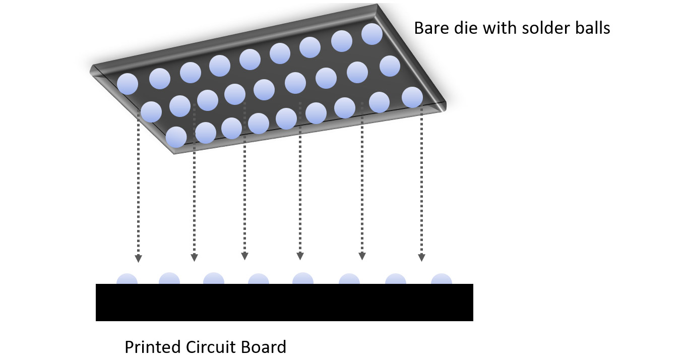
A bare die with solder balls showing how the balls are aligned to connections on a printed substrate
What is the Chip-on-Board Process?
Chip-on-Board (CoB) is simply a specialized process for attaching integrated circuit chips to any given substrate or board. With the wide variety of technological devices being developed, the size and shapes of both the IC and the substrate vary drastically by product. We must use advanced electronic assembly techniques such as CoB to make these products come to life.
Difficult as it is to design processes for assembling tiny, powerful chips, we can't move forward without them. With Qualcomm announcing their new Snapdragon Ride System-on-Chip (SoC) processing core that provides a range of autonomous vehicle support, the industry is counting on manufacturers to integrate these chips successfully. Chip-on-Board is one of the advanced electronic assembly processes we'll use as devices continue to require more functionality in increasingly smaller formats.
The Future of Miniaturization
Admittedly, Gordon Moore's law about cramming more components onto integrated circuits seems to be slowing when you consider the cadence of chip manufacturers' release of their next smallest transistor node chips. Intel themselves hit a few slowdowns when they approached the single digit nano-scale transistor nodes. And now, manufacturers are faced with even greater delays thanks to global supply chain shortages of essentially every type of component.
However, researchers are already looking into different approaches to execute the switching or routing task typical of a transistor. In essence, researchers are looking to control this signal routing with transistor-like devices that would be in the nano and sub-nanometer scale.
Research has shown promising results with the use of organic transistors, specialized materials like ferroelectric transistors and even quantum transistors that would require entirely different hardware and disrupt the electronic landscape as we know it today. And as these new transistor-like devices evolve, it is our advanced assembly teams that will make it possible to incorporate them into products at scale across the globe.
With miniaturization, researchers hope to solve some of humanity's biggest problems. Brilliant new breakthroughs from the world's most respected research institutions promise longer, healthier lives and cleaner energy that will power everything from autonomous vehicles to spacecraft and everything in between. But without advanced electronics assembly, this research will not find its way to consumers.
Advanced electronics assembly brings research to life, finding ways to fabricate at scale, minimizing costs and leveraging massive engineering expertise. Whether you're a startup or a Fortune 500 technology leader, if you're creating the next disruptive electronic device, an advanced electronics assembly team can help you go seamlessly from prototype to production, no matter how tiny or complex the electronics.
Follow the Jabil Blog
Sign up for weekly updates on the latest trends, research and insight in tech, IoT and the supply chain.

